Physicists engineer ferroelectricity into well-known family of semiconductors
Overall technique could be applied to other materials
MIT physicists and colleagues have engineered a new property into a well-known family of semiconductors by manipulating ultrathin sheets of the materials only a few atomic layers thick.
The work is important because the new materials themselves could have interesting applications in computing and more. In addition, the overall approach is generic and can be applied to other pre-existing materials, expanding their potential applications as well.
Semiconductors are materials like silicon with conductivity somewhere between metals, which allow electrons to move very efficiently, and insulators (like glass) that stymie the process. They are the cornerstone of the computing industry.
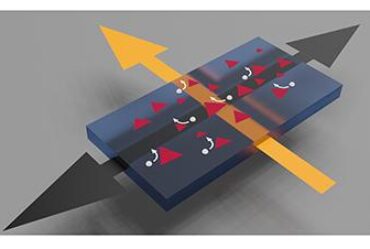
The semiconducting materials involved in the current work are known as transition metal dichalcogenides (TMDs). The MIT team showed that when two single sheets of a TMD, each only a few atomic layers thick, are stacked parallel to each other, the material becomes ferroelectric. In a ferroelectric material, positive and negative charges spontaneously head to different sides, or poles. Upon the application of an external electric field, those charges switch sides, reversing the polarization. In the new materials, all of this happens at room temperature.
TMDs are already well-known for their interesting electrical and optical properties. The researchers believe that the interplay between those properties and the newly imparted ferroelectricity could lead to a variety of interesting applications.
“Within a short time, we have managed to vastly expand the small, but growing, family of two-dimensional ferroelectrics, a key type of material at the frontier in applications in nanoelectronics and artificial intelligence,” says Pablo Jarillo-Herrero, the Cecil and Ida Green Professor of Physics and leader of the work, which was reported in Nature Nanotechnology. Jarillo-Herrero is also affiliated with MIT’s Materials Research Laboratory.
In addition to Jarillo-Herrero, authors of the paper are Xirui Wang, an MIT graduate student in physics; Kenji Yasuda and Yang Zhang, MIT postdoctoral associates; Song Liu of Columbia University; Kenji Watanabe and Takashi Taniguchi of the National Institute for Materials Science, in Japan; James Hone of Columbia University, and Liang Fu, an associate professor of physics at MIT.
Ultra-Thin Ferroelectrics
Last year Jarillo-Herrero and many of the same colleagues showed that when two atomically thin sheets of boron nitride are stacked parallel to each other, the boron nitride becomes ferroelectric. In the current work, the researchers applied the same technique to TMDs.
Ultra-thin ferroelectrics like those created out of boron nitride and TMDs could have important applications including much denser computer memory storage. But they are rare. With the addition of the four new TMD ferroelectrics reported in Nature Nanotechnology, all part of the same semiconductor family, “we’ve nearly doubled the number of room-temperature ultrathin ferroelectrics,” says Xirui Wang. Further, she noted, most ferroelectric materials are insulators. “It’s rare to have a ferroelectric that is a semiconductor.”
What’s Next?
“This is not limited to boron nitride and TMDs,” says Kenji Yasuda. “We’re hopeful that our technique can be used to add ferroelectricity to other pre-existing materials. For example, could we add ferroelectricity to magnetic materials?”
This work was funded by the U.S. Department of Energy Office of Science, the Army Research Office, the Gordon and Betty Moore Foundation, the U.S. National Science Foundation, the Ministry of Education, Culture, Sports, Science and Technology (MEXT) of Japan, and the Japan Society for the Promotion of Science.


